I’ve been working on a project and needed a prototype printed circuit board to get the project looking a little more finished and less of a mess of wires on a prototyping board. I decided to use the photo sensitive method for the PCB as well as for the solder mask with reasonable results.
I laid the board design out in Eagle which wasn’t the easiest thing as I normally use KiCad for PCB design, so there was a bit of a learning curve but it’s good to try different things. I certainly like Eagle’s large collection of parts libraries to make things easy, but I can whip new parts together in KiCad in just a few minutes.
After going through the schematic design and PCB layout, I printed out the appropriate layers for the top and bottom side of the board. For the top side these were the top copper, vias and pads and for the bottom layer the bottom copper, vias and pads.

I printed these out on copier transparency film in black and white on a color laser printer to get the highest density possible on the toner. When you expose these boards, if the toner is thin, the UV light will penetrate it and expose the resist on the traces resulting in excessive pitting and damage to traces.
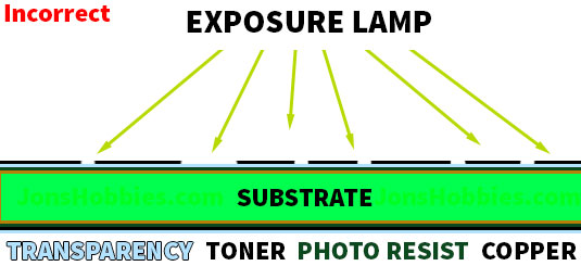
The top layer has to be mirrored before it’s printed to the transparency, the reason for this is that you want the side of the transparency with the toner (the side that looks flat and not shiny) to be pressed firmly against the blank board during exposure. Here’s a photo of the back transparency I used and the difference between the flat and shiny side.

If you imagine the sandwich with the PCB substrate and copper, photosensitive material atop of that, the toner and the transparency, your stack looks something like the following image, and blocks incident light pretty well.
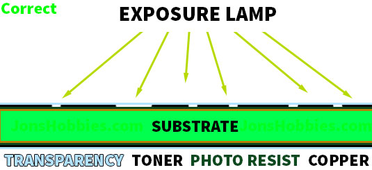
If you layup your board so that the toner is on the very top, the light can leak in under the transparency and ruin the sharpness of your traces and it may make fine pitch traces very difficult to achieve. in the drawing below you can see how the transparency creates a light gap beneath the toner.
I used MG Chemicals 600 Series Positive Presensitized Copper Clad Board with 1 oz Copper, 1/16″ Copper Thick, 2 Side, 6″ Length x 6″ Width, FR4 for the circuit board. I sliced off a smaller piece to use with the dremel, but a hacksaw or shear works as well.
Since this is a double sided board and the two transparencies need to be aligned I drilled 2 of the component holes while the protective film was still on the PCB material. This allowed me to align the top and the bottom board transparencies to the holes so that I would get pretty good front to back alignment. There are many ways to align the sheets and this is just one of them. Other people use a frame with pins and punch holes to in both transparencies once they are aligned. When producing the job, the transparencies align to the pin in the frame. That method is also very common in production shops.
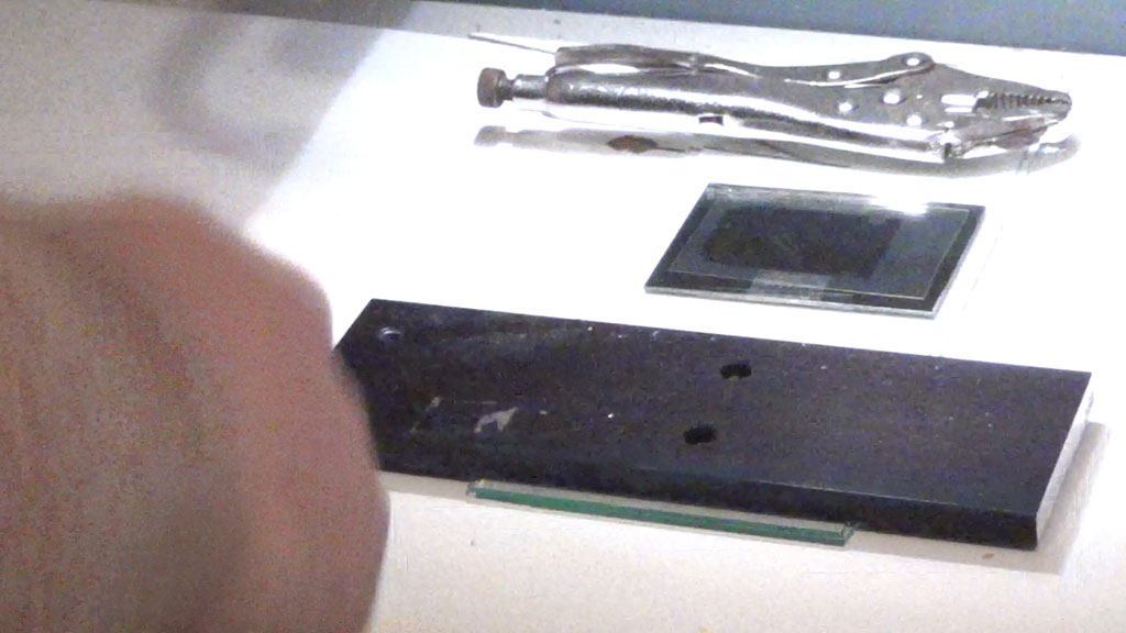
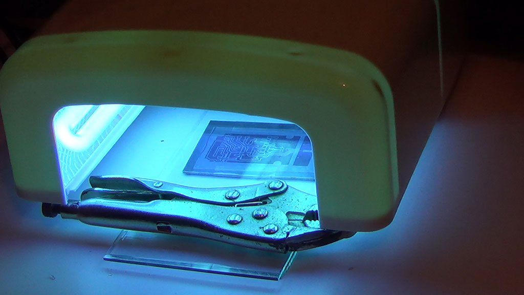
Once the transparencies were aligned and taped onto the positively sensitized printed circuit materials I weigh down a glass plate over the transparencies to hold them tight to the board and exposed them with an ultraviolet light. I had been using a 500 Watt halogen lamp with the front glass removed. The front glass has a UV filter, and without this the halogen bulb puts out a significant amount of UV light to expose the board. My exposure times with this lamp were anywhere from 1m45s to 2m flat. Unfortunately the bulb failed in this exposure, so I switch to a UV nail curing light, it was also able to develop the board in 2 minutes.
Here’s a frame from the video that shows the bulb just as the filament breaks, it got quite bright for a very brief moment of time. On the top part of the PCB you can see a very bright spot, this is a reflection of the arc inside of the halogen lamp as the filament separated.
 As mentioned I switched to the UV nail drying station I bought on eBay for about $25USD to expose the PCB and everything worked out just fine for that. 2 minutes per side and the board was well exposed.
Once the board was exposed on both sides I removed the transparencies and dipped the board into the developer which is MG Chemicals 418 Positive Developer, which is really just sodium hydroxide. (Sodium hydroxide is hazardous, take all precautions, wear eye protection and gloves at all times it is in the open! Make sure to read all safety precautions and follow instructions.) The developer is mixed at a 10 parts water to 1 part developer ratio and is very fast acting.
You have to make sure that all exposed areas are clean if photo-resist down to the copper with no haziness or fog on the clear copper areas, but at the same time you don’t want to start losing the photo-resist you want to keep. Keep a very close eye on the developing process and then rinse thoroughly with water as soon as it’s done to stop development.
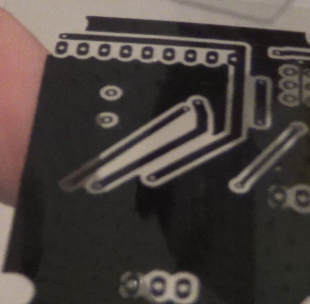
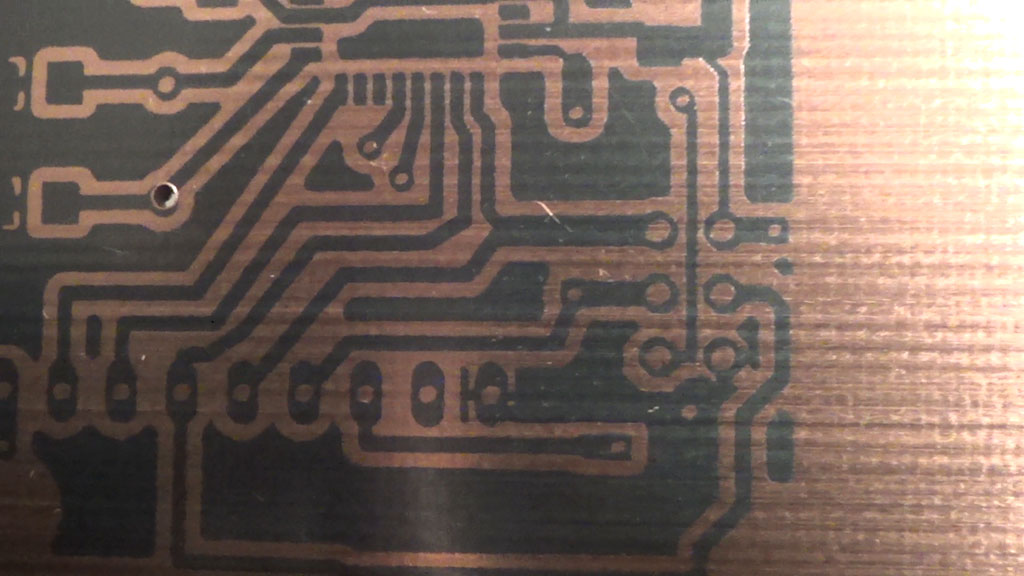
This is what my board looked like after less than 45 seconds in the developing tank.
The next step is to etch the excess copper plating off of the circuit board. There are a few options for this but all of them create a solution which has copper dissolved in them. Copper is unhealthy for the environment and a hazard to fish, so whichever method you choose to use, you will need to find a way to properly dispose of it. Copper etchants will also damage any copper plumbing and are still active, even if you think your solution is spent. While many homes use PVC drains these days, the P trap pipe under the sink may be chrome plate brass or nickel. PCB etchant of any type can be re-used multiple times before it’s ‘spent’.
In my case, I used ferric chloride to etch the circuit board. It’s readily available at Radio Shack or through online vendors and can be disposed of in multiple safe ways such as residential toxic waste pickup/drop off program through your municipal waste authority, or by fully neutralizing the solution with baking soda, drying it and then disposing of it as dry waste.
Like with the developer you should wear gloves and eye protection. While the ferric chloride doesn’t fume a lot or release noxious fumes at high levels, under normal circumstances, this should be done outdoors or in a well ventilated area. Ferric chloride will stain everything it comes in contact with.
With all that out of the way, I dumped the board in the etchant and let it go for a while, the etchant was cold and it was taking too long (A slow etch can undercut your traces) so I heated up the ferric chloride by putting the glass jar in a pan full of hot tap water, this heated it up and sped up the process.

Depending on the temperature of the etching solution, after anywhere from 10-20 or more minutes you will have a completely etched circuit board. You can slosh the container to speed the etching process, but wear gloves, eye protection (you should anyways when working with chemicals) and cover the top of the container with a paper towel or napkin.
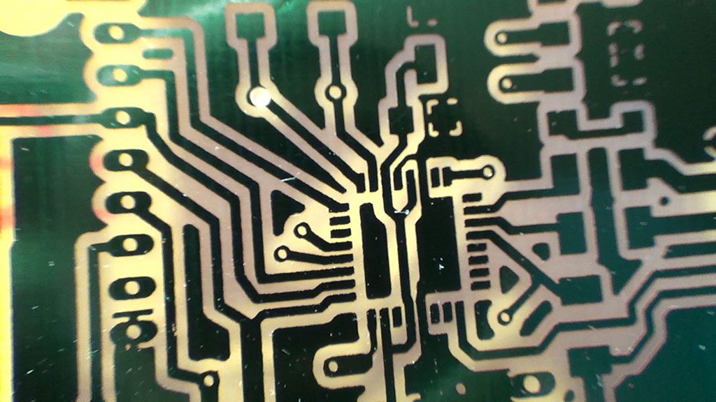
After all of the useless copper is removed from the printed circuit board rinse it off well under water to halt the etching process. I made sure to rinse it off very well and then dry it, even very dilute ferric chloride can continue to etch your copper while your board sits around.
The next step was to add a solder mask layer to the board. The solder masking has a few purposes. When boards were/are wave soldered in a bath of molten solder, the solder mask would cover large areas of exposed copper to prevent solder from sticking to them and only soldering where components were. This saved a lot of solder. I you want to beef up the ampacity of a conductor, then you’d want to leave the solder mask off. A solder mask also helps prevent component conductors from getting soldered together by accident. Finally, the solder mask adds a nice finished look to any board, or more finished than a raw board and it helps prevent the unplated copper from oxidizing. For hobbyist prototypes it’s certainly not a requirement but a nice addition.
The solder mask will be covered in part 2, or, if you want the basic information now, watch the complete video below. Please make sure to like/thumbs up, or comment if you have any questions, it helps me in the long run to produce more content and better quality videos.
1 responses to DIY Printed Circuit Board With Solder Mask – Part 1
Hi Jon!
I’m trying to do a pcb with gap in the pads, but only in one of two copper layer.
I select the gap option in pcbwizard and it put in the two layers(Top and Botton).
I can’t put the gap only in one copper layer. Do yo know an option in eagle or KiCad?
Thanks!!
Leave a reply to DIY Printed Circuit Board With Solder Mask – Part 1